
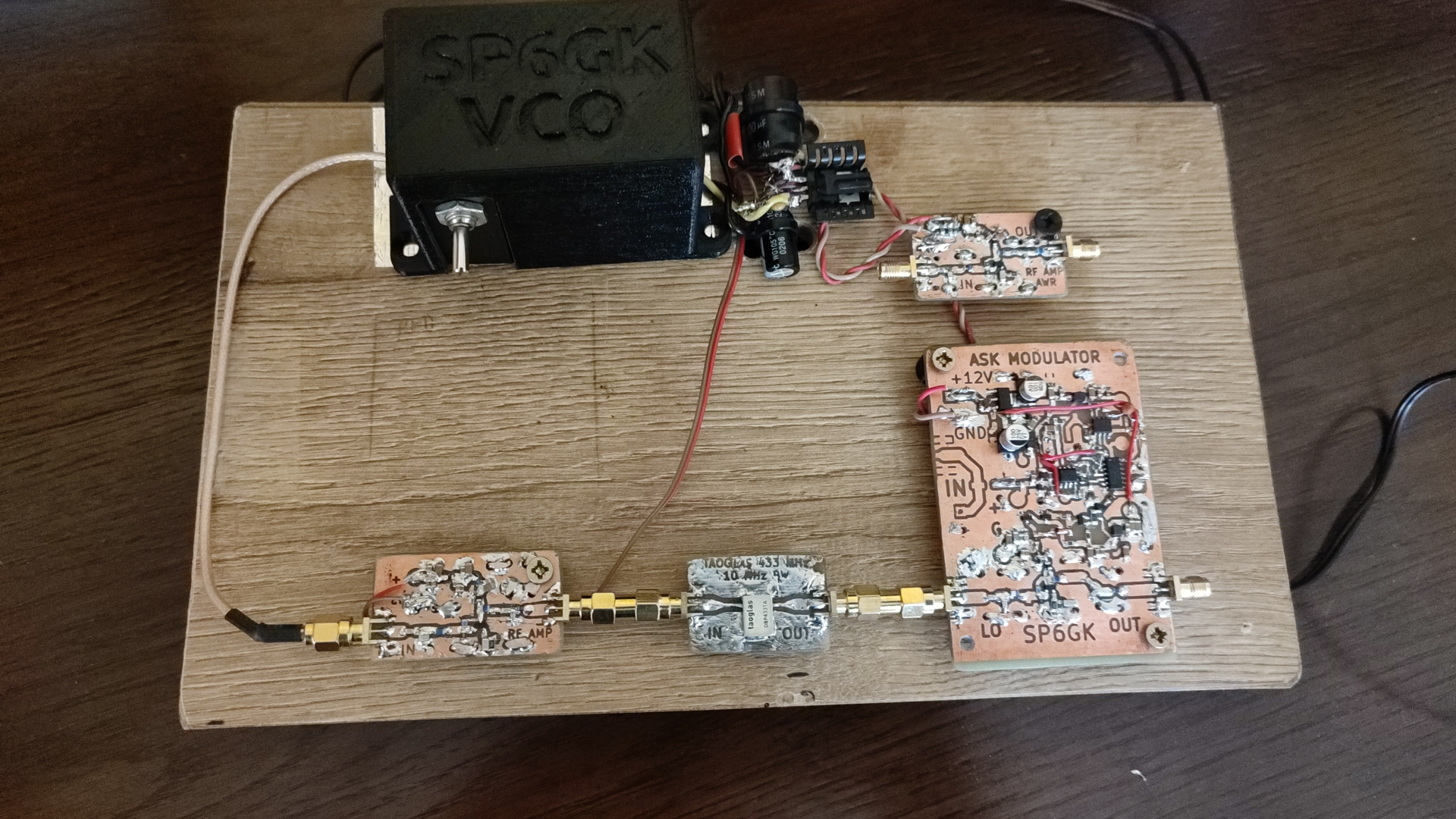
It seems that nowadays, the most difficult part of sending data from a sensor to a remote device is choosing a protocol. With off the shelf Bluetooth, Wi-Fi, Zigbee, and LoRa modules and libraries readily available, the possibilities seem endless. But what about the underlying physical hardware at the lowest layer of the network stack? I decided it would be a fun exercise to implement a digital transmitter from the ground up, without using any ASICs or microcontrollers. I set myself the task of constructing a device that would transmit data from an analog 0–5 V sensor at 433 MHz. The result is a simple Amplitude Shift Keying (ASK) transmitter.
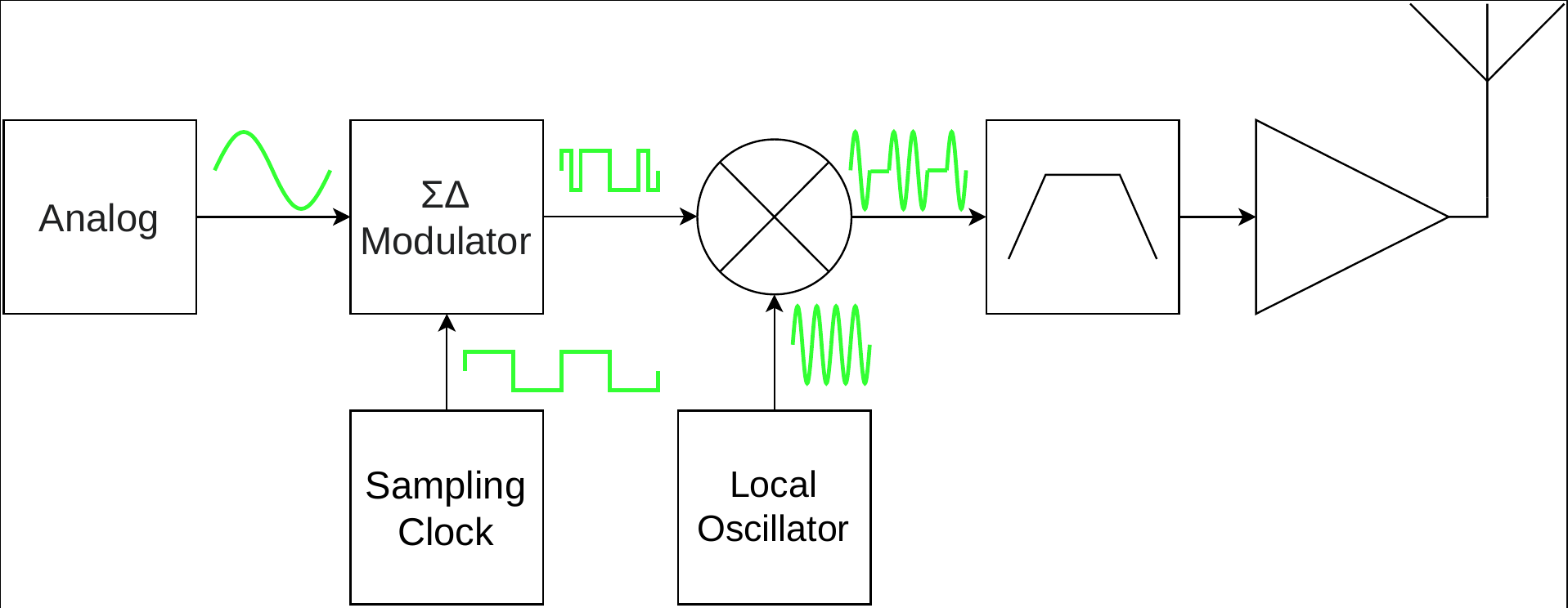
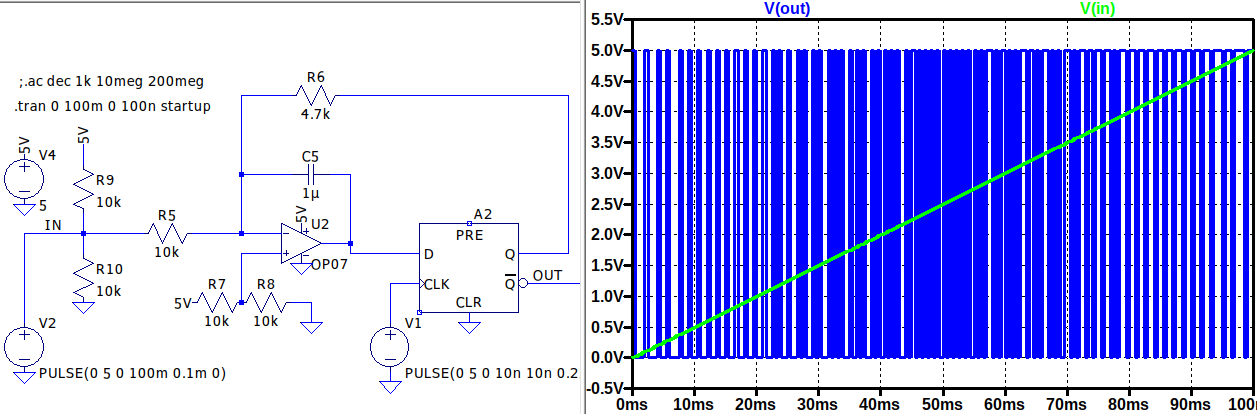
The transmitter is built around a first order sigma-delta modulator. Sigma delta modulation is a type of analog to digital conversion (ADC) commonly used in microcontrollers and basic audio equipment. At the hardware level, it is a one bit ADC that uses oversampling and noise shaping to achieve conversion. At the heart of the circuit is a comparator based on an op amp (U2A, LM358), which essentially acts as a one bit ADC. This comparator drives a D type flip flop (U1A, 74HC74) that generates a pulse width modulated signal with a frequency determined by a sampling clock generator. In modern systems, this clock can run at very high frequencies (even hundreds of MHz, which is how a high effective number of bits can be achieved). Here, however, for simplicity of debugging and demonstration, a very slow clock of 200 Hz is used.
The clock is generated by the legendary 555 timer (U3). The output from the sigma delta modulator is a bitstream in which the pulse density is proportional to the amplitude of the input signal. This waveform is then buffered by a common emitter amplifier (Q11), which converts the signal from 5 V logic levels to 12 V. This signal then drives a keyer circuit. Two level ASK can be viewed as a binary form of classical amplitude modulation (AM). This particular case is also referred to as On Off Keying (OOK). Therefore, the baseband signal (the output from the sigma delta modulator) is upconverted by a mixer that is essentially a binary switch, usually referred to as a keyer. The origins of this modulation technique date back to the early days of telegraphy. The keying speed (the rise and fall times of the carrier signal) determines the bandwidth. Higher modulation speeds come at the cost of increased bandwidth. Since we want to avoid interfering with other devices in the already crowded 433 MHz band, a circuit that slows down the rise and fall times of the 433 MHz carrier is used. This circuit was adapted from Experimental Methods in RF Design, published by the ARRL. The keyer essentially modulates the supply voltage of an RF amplifier built around a BFR92P transistor (Q2). This amplifier is matched for 433 MHz operation and presents a 50 Ohm impedance at both the input and output (the design is described here).
These days, generating a stable signal with low phase noise is simpler than ever, thanks to phase locked loop (PLL) ICs with integrated voltage controlled oscillators (VCOs). But where is the fun in programming the divider registers again and again?
Let's generate the carrier the old fashioned way. Generating a 433 MHz signal directly using an LC oscillator based on discrete components is not easy due to frequency instability and parasitic effects. Therefore, the initial signal is generated at one third of the target frequency, or approximately 144 MHz. To generate this signal, a VCO capable of tuning from approximately 120 to 180 MHz is used, resulting in coverage of the 360–540 MHz range after frequency multiplication.
Open loop VCOs might appear to be simple devices based on their schematics, but in reality, they need to be constructed very carefully. Oscillators operating at such frequencies are highly susceptible to frequency drift caused by temperature changes and even the proximity of nearby metal or ferromagnetic objects. The load type can also affect the center frequency (the pulling and pushing effects). Input voltage and control voltage have an effect as well. To mitigate these effects, several measures were taken:
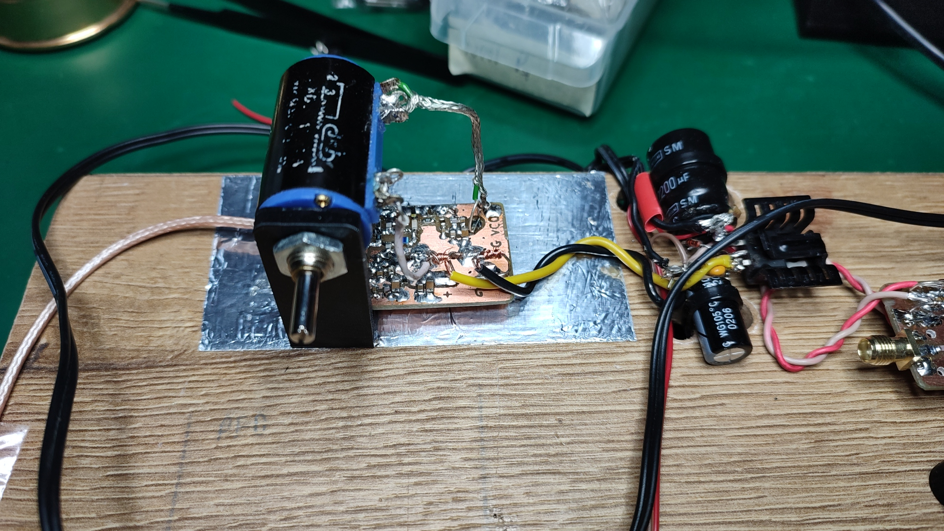
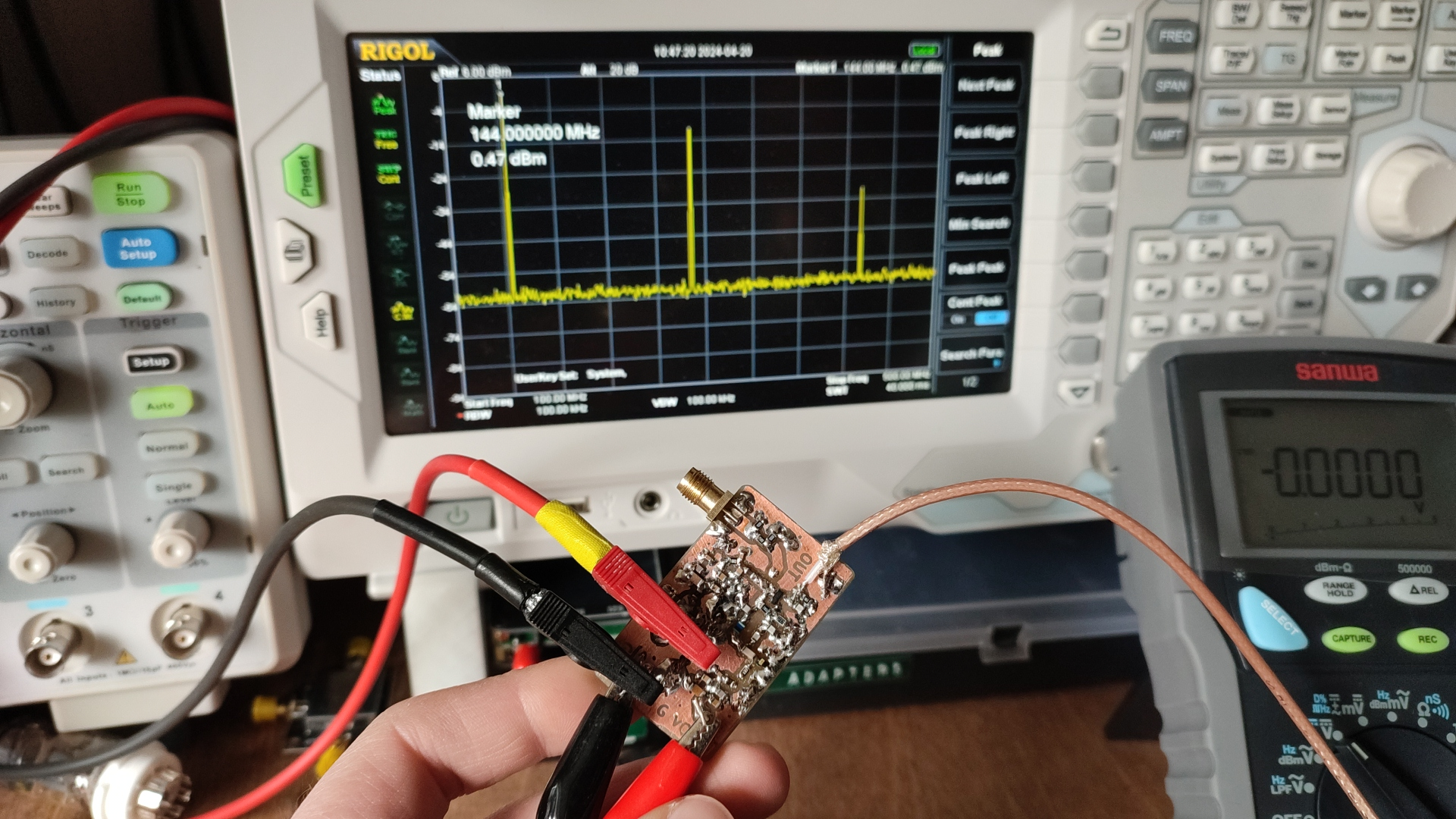

Better stability could be achieved using a crystal resonator, most likely operating at its overtone frequency. For more serious applications, one can also buy a ready made VCO from companies such as Mini-Circuits. These come with various tuning ranges and tuning sensitivities, but building your own can teach you not only the basics of how such a circuit works and what its limitations are, but also give you a greater appreciation for professional VCO designs.
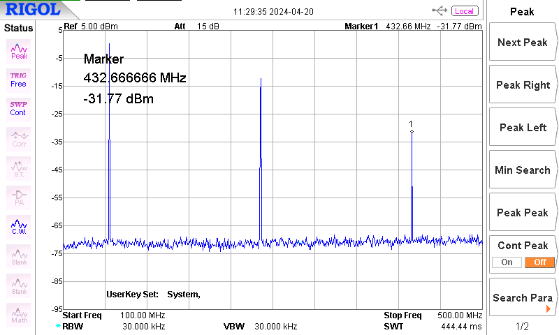
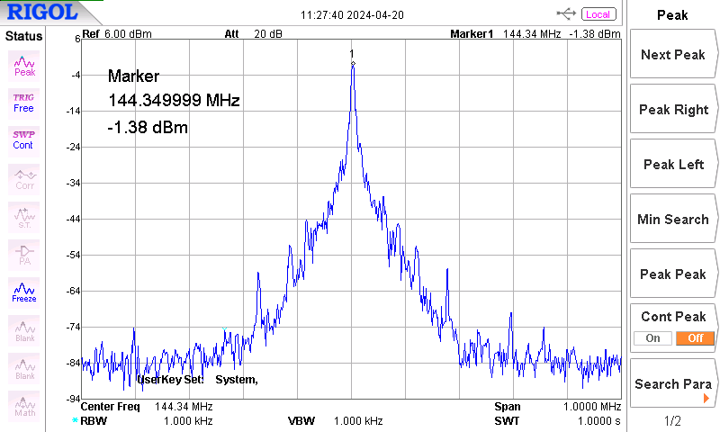

It can be seen that shielding has drastically improved the phase noise of the VCO. This effect is easy to observe with an exposed VCO circuit: simply blowing on it causes a noticeable frequency shift due to changes in temperature. The same phenomenon occurs on a much smaller scale during normal operation. The frequency shift is not as large, but it still manifests as additional modulation of the carrier. Phase locked loops compensate for such effects using very fast and wide feedback loops, but that is a topic for another project.
It can also be seen that while the fundamental signal at 144 MHz is around -1.4 dBm, the signal at 433 MHz is much weaker, at -31.8 dBm. In the next stage, we will use a tuned 433 MHz amplifier followed by a 433 MHz band pass filter to select only the desired signal. This amplifier is used not only to select the desired frequency but also to provide isolation between the VCO and the keyed amplifier. Since the keyed amplifier is switched on and off, its impedance constantly changes between 50 ohms and some other value. These impedance changes can affect the VCO's frequency. Further improvements in isolation can be achieved through passive impedance matching, such as using an attenuator, since the added insertion loss improves the return loss. A Taoglas off the shelf ceramic filter was chosen as the band pass filter and mounted on a homemade PCB.
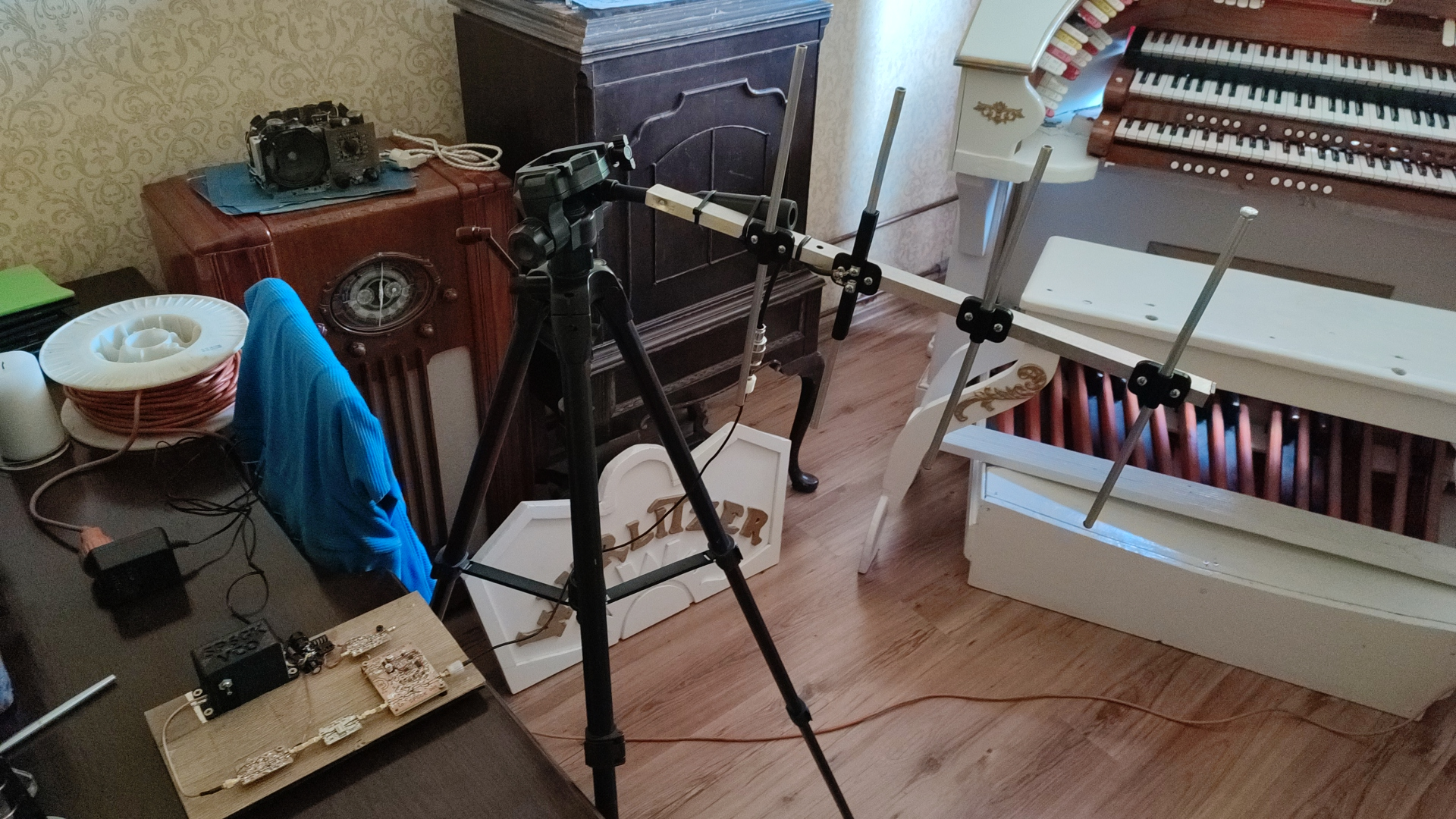
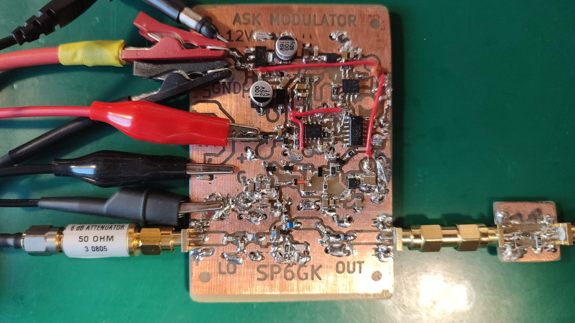
All PCBs used in the transmitter were etched using methods available at home. A single-sided layout was sufficient, with three additional traces on the top side implemented using wires. Because the transmitter's output was not very clean, an output amplifier was omitted during testing. The receiving setup consisted of my SDR receiver (Rhapsody SDR) with an external ADE-25 mixer driven by an ADF4351 PLL as the local oscillator. An RTL-SDR V3 dongle was used as an alternative receiver. A quarter wavelength vertical antenna was used on the receiving side. On the transmitting side, a four-element Yagi-Uda antenna was used in vertical orientation. The setups were placed in separate rooms, with line of sight between them and a distance of approximately 5 m.
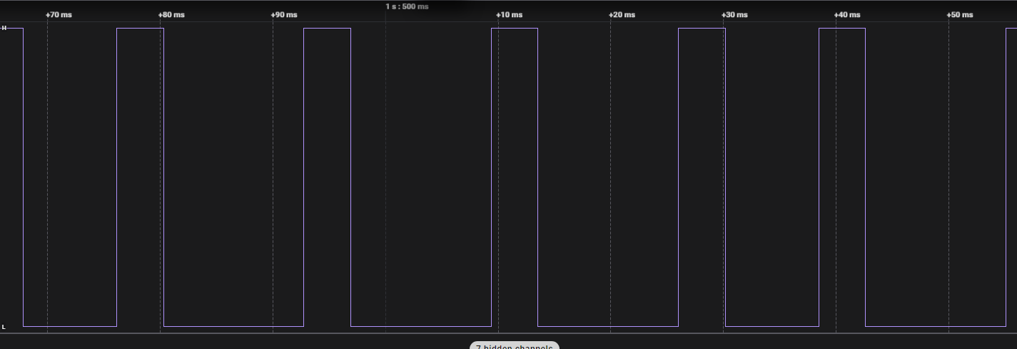
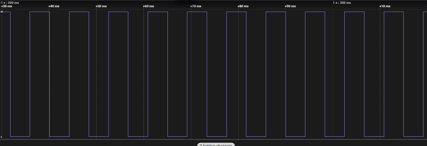
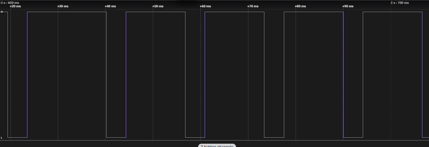
First, the modulator output (the PWM signal used to key the RF section) was tested using a logic analyzer. By applying 0 V, 2.5 V, and 5 V to the transmitter input, different waveform patterns were observed, confirming that the modulator was working as expected.
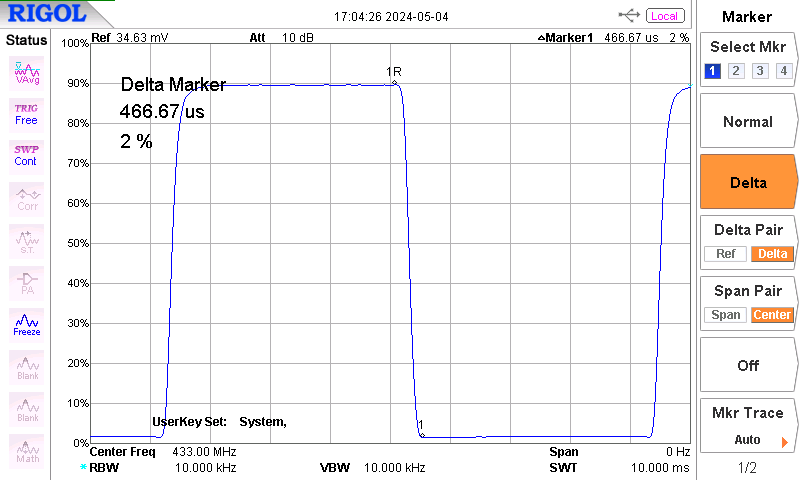
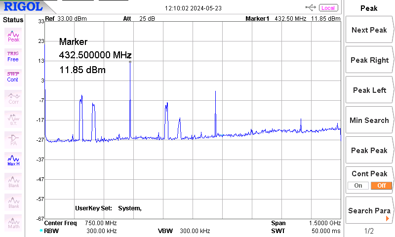
The transmitter output was observed using a spectrum analyzer.
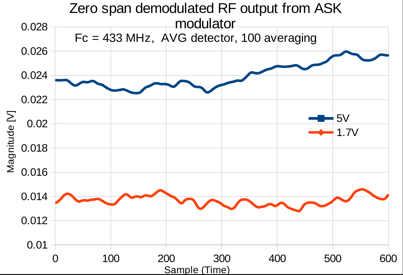
The most interesting measurement here involved using zero span mode, which turns the spectrum analyzer into a selective oscilloscope. In this mode, the spectrum analyzer does not sweep across the spectrum. Instead, it remains tuned to a single frequency and plots the detected RF level over time. The advantage of this approach is that it retains the high selectivity provided by the resolution bandwidth (RBW) filters.
Since the pulse width in our ASK signal is proportionally related to the input voltage, the average RF level measured in zero span mode at 433 MHz should also be related to the transmitter's input voltage. Indeed, this relationship was confirmed, demonstrating that the transmitter fulfills its intended purpose.
The output spectrum is not particularly clean. However, part of the problem, identified while analyzing these results some time later, might have been that the signal level at the spectrum analyzer's mixer was too high. (Yes, staying within the safe input level does not necessarily mean that the mixer itself is not being overdriven.)
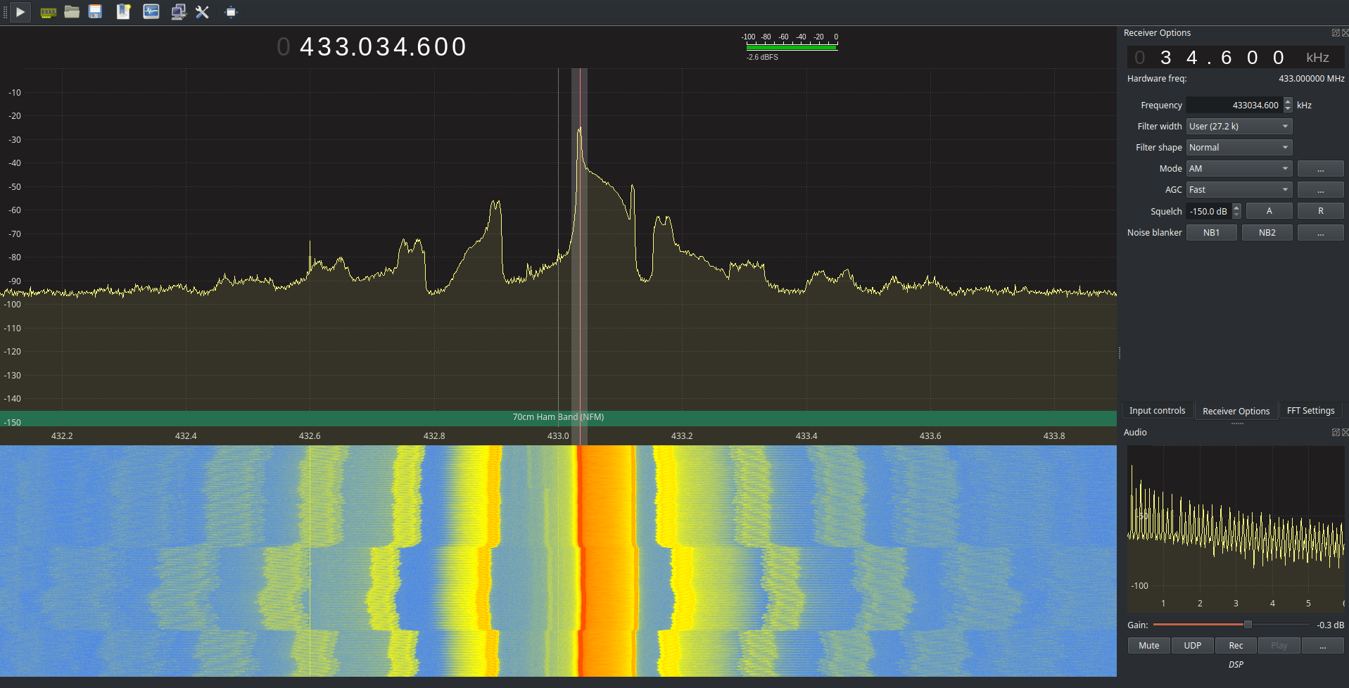
Finally, differences in the received signal corresponding to three input voltages were observed using the SDR's audio output and SSB demodulation. Notice that, in the photo of the receiving setup, the trailing phase noise appears inverted in the waterfall display compared with the GQRX screenshot from the RTL-SDR at the top of this website. This is because low side injection was used for downconversion, which inverts the spectrum.
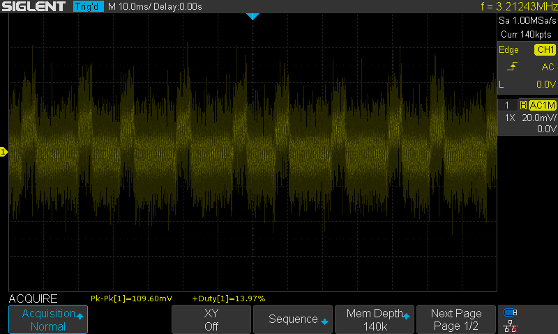
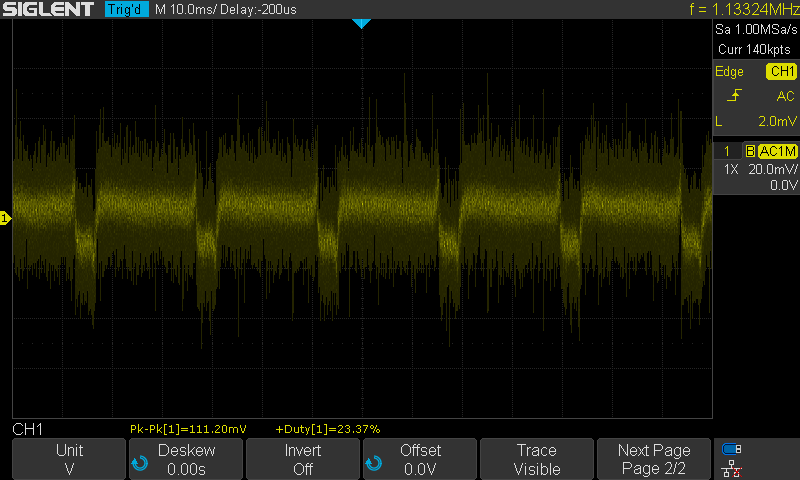
In conclusion, a complete ASK transmitter was designed, simulated, assembled, and tested. The project is highly modular, with home-etched PCBs mounted on a piece of floorboard. A method of generating UHF frequencies without using a PLL was demonstrated by selecting harmonics of a VCO operating in the VHF range. Methods for analyzing phase noise and frequency stability were discussed, and solutions to mitigate these problems were introduced. Modern test equipment was used to evaluate the assembled system. Although the transmitter emits significant spurious emissions, the output at 433 MHz correlates with expectations. While not particularly practical, the presented project provides a good learning platform for multiple areas of RF design.
sp6gk 'at' protonmail.com
Here is demonstration of a restored radio from 1938.
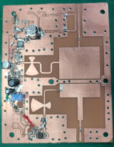
Almost assembled fully home made 2.4 GHz power amplifier on LDMOS transistor.
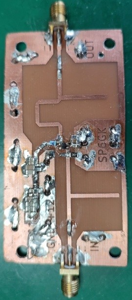
1.25 GHz small signal amplifier with open stub matching. Active element is BFP420 BJT.

My 120 cm prime focus dish. For now in the feed I have the Bullseye LNB. Thanks to my home made bias Tee and polarization controller I can receive the QO-100 satelite just fine on the RTL-SDR. Now I am working on upconverter and 2.4 GHz PA for the uplink.